Date: Thu Feb 10 2011 - 09:12:00 PST
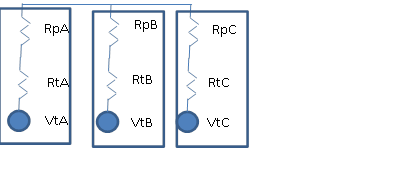
The state is maintained by the capacitive drivers. Consider the scenario below. Three drivers, A, B, and C in three different modules. Each module must also have a parameter to drive an additional parasitic. Any parasitic resistance with three devices or less can be accurately modeled with a distributed parasitic, since there is always a single "common point" on a wire with three taps. For larger numbers of taps, such a configuration may only be an approximation.
Regardless, the capacitor charge state is maintained with VtB and VtC, and the appropriate time steps are controlled by them. When they see a large slew rate, they can adjust their time-steps appropriately. When the slew rates are reduced, they can reduce their time steps. I don't know what the performance penalty is versus a centralized "resolution" module, but I don't think it's large.
[cid:image001.png@01CBC90E.2CE2FE70]
An alternative approach is for the netlist to instantiate discrete resistors and/or capacitors in the interconnect. The efficiency of a large number of discrete devices versus a centralized "resolution" module is not clear.
Finally, if efficiency demands a centralized module for the interconnect, the netlist can simply instantiate an interconnect module in a flattened netlist, as I described in an email sent out earlier today. The problem with this is that one loses the hierarchical structure. Functionally, it provides everything you want.
-----Original Message-----
From: owner-sv-dc@eda.org [mailto:owner-sv-dc@eda.org] On Behalf Of Achim Bauer
Sent: Thursday, February 10, 2011 8:51 AM
To: sv-dc@eda.org
Subject: [sv-dc] resolution function with a state ?
Hi,
following I describe a simple and common scenario for real-value or logic resolution. I am not sure if our current resolution methodology can handle this efficiently.
Lets consider logic values first:
we have a driving gate A (VDD=1.2V), two loading gates B (VDD=1.8V) and C (VDD=1.0V) and a common net "n".
Lets assume "A" has driven a "0" for a while and suddenly drives a "1".
"A" shall have a driving strength of 1/10k(Ohm) and "B" and "C" load with altogether 100f(F).
In that case the RC-constant of the common net is 10kOhm*100fF = 1ns and thus the slew rate is 1.2V/1ns = 1.2GV/s.
A resolution module might simply schedule a "1" for "B" within 1.8/2/1.2G s = 0.75ns and a "1" for "C" in 1.0/2/1.2G s = 0.42ns.
A resolution function that is exclusively based on Norton/Thevenin equivalents and has no intrinsic state and timing for "n" would have to render this inertial behavior by a sufficiently large number of time steps within the connected Norton/Thevenin equivalents (provided there is a way to determine the appropriate time step for "n").
Basically the same applies if we take real-value drivers and readers/loads instead of logic.
So the resolution MODULE would be more accurate and 10-100x faster than a resolution FUNCTION. A resolution module would also allow to easily attach an initial value to a net and it can be the right place to take care of an optimum timing for triggering and reevaluating the Norton/Thevenin equivalents.
These are some of the reasons, why I think a resolution MODULE with intrinsic state and timing might be a better methodology for practical application.
Please let me know about your opinion.
Thanks,
Achim
--
This message has been scanned for viruses and dangerous content by MailScanner, and is believed to be clean.
--
This message has been scanned for viruses and
dangerous content by MailScanner, and is
believed to be clean.